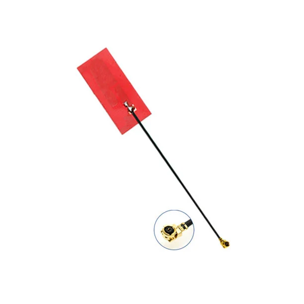
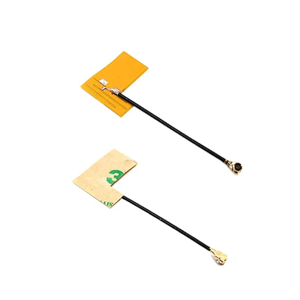
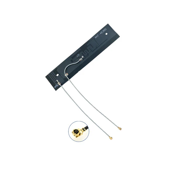
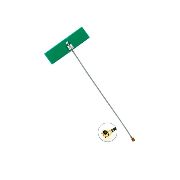
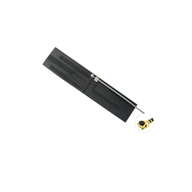
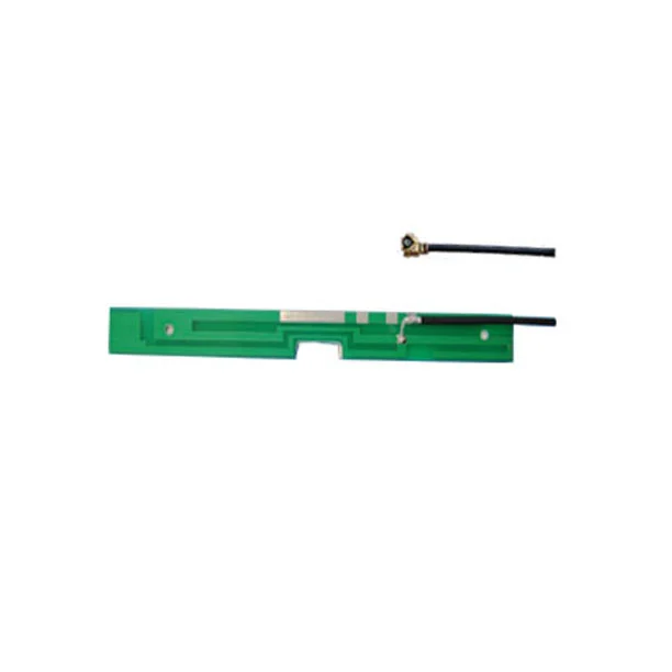
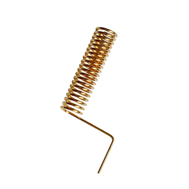
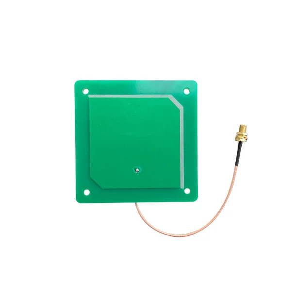
At Asian Creation Communication, we manufacture PCB antennas with a focus on reliability, compact design, and RF performance for global OEM and embedded device applications. Our PCB antennas cover frequency ranges that include 433 MHz, 868 MHz, 2.4 GHz, 5.8 GHz, and custom bands up to 6 GHz, supporting Bluetooth, Wi-Fi, NFC, LoRa, and GPS/GNSS.
Materials & Substrate Selection
We commonly use FR4 substrate for cost-effective designs; for higher frequency or performance requirements, we also offer Rogers or PTFE-based materials to improve performance (lower loss, better stability). Trace thickness, copper weight, and ground plane dimensions are optimized to achieve a VSWR of < 2.0 (typically ≤1.8 in many products).
Performance Parameters
Gain: typically between −2 dBi (for small chip/trace antennas) up to 6–8 dBi (for larger patch-style PCB antennas) depending on frequency and layout.
Bandwidth: Many designs support bandwidth ratios of up to 4:1 (e.g. 1.8 GHz to 7.2 GHz), depending on trace layout and matching.
Polarization: Vertical, horizontal, or dual (depending on the device requirement).
Efficiency: Typical designs achieve >60% antenna efficiency at mid-band frequencies under optimal board layout.
PCB Layout & Installation Tips
1. To ensure optimal PCB antenna performance, we recommend:
2. Keeping the antenna trace away from metallic components and power lines — spacing of at least 5 mm (or as per design) where possible.
3. Designing a sufficient ground plane — board area under and around the antenna equal or greater than certain dimension (e.g. 30 x 30 mm or more for higher frequency bands).
4. Performing impedance matching tuning — using matching stubs or networks to reduce VSWR and maximize power transfer.
5. Environmental considerations — ensure protective coating or conformal coating if exposed to humidity or temperate extremes.
Manufacturing & OEM Services
ISO 9001 certified production with continuous incoming inspection, in-line QC, and finished product inspection.
Sample lead time: typical 7–10 days for standard PCB antenna models; custom designs: 2-3 weeks for prototype.
MOQ: starting from 200-500 pieces, depending on complexity and frequency.
Application Use Cases
Embedded in smart home gateways and routers where PCB antennas provide internal wireless coverage.
Wearable / IoT sensors, remote monitoring devices using 868 MHz / LoRa bands.
NFC, RFID tag readers where small PCB trace antennas are essential.
GPS/GNSS receivers with embedded patches or stub antennas printed on PCB for form-factor devices.


 English
